Chinese Scientists Develop Rapid 3D Optical Structure Fabrication Method
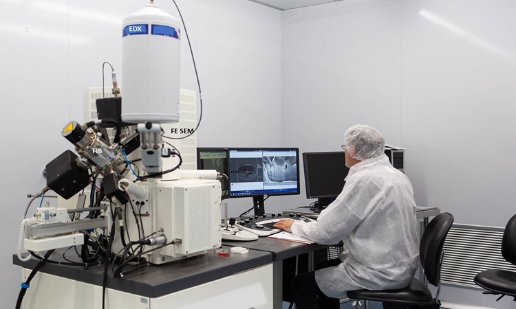
Chinese scientists have introduced a novel parallel fabrication method capable of transforming 2D models into complex 3D optical structures across entire semiconductor wafers in mere seconds. This breakthrough significantly accelerates the production process for optical components. The technique allows for the rapid creation of intricate three-dimensional designs on semiconductor materials, a process that traditionally takes considerably longer. By enabling parallel processing, the method enhances efficiency and scalability in chip manufacturing. This advancement is expected to have a substantial impact on the speed and cost-effectiveness of producing optical chips. The researchers aim to further refine this technology to meet the growing demands of the semiconductor industry. The development represents a significant step forward in China's efforts to advance its domestic chip production capabilities.
This technological advancement in semiconductor fabrication addresses critical bottlenecks in optical chip production by drastically reducing fabrication time from hours or days to seconds. The parallel processing approach leverages computational efficiency to create complex 3D structures, potentially lowering manufacturing costs and increasing throughput. This innovation aligns with global trends in accelerating technological development and could position China to capture a larger share of the advanced semiconductor market. The long-term implications include enhanced competitiveness in areas requiring sophisticated optical components, such as telecommunications, artificial intelligence, and advanced sensing technologies. Further research will likely focus on the scalability, yield rates, and integration of this method into existing manufacturing workflows.
AI-generated to prompt reflection — not editorial opinion, not advice, not a statement of fact. How this works.