Chinese Scientists Develop Rapid Chip Manufacturing Technique
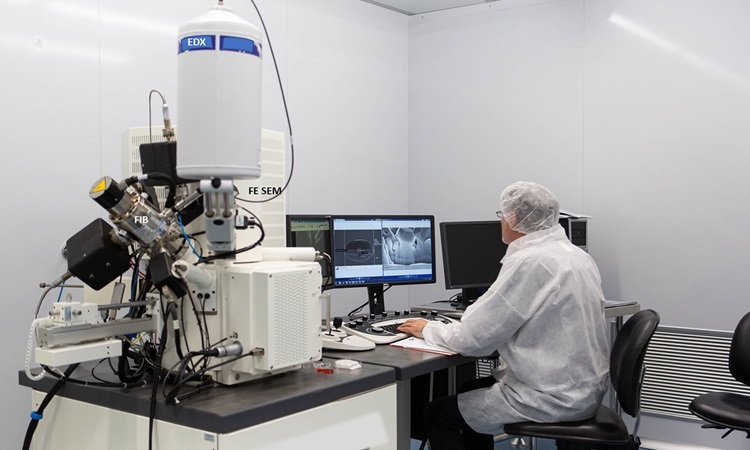
Chinese scientists have introduced a groundbreaking parallel manufacturing method that significantly shortens the production time for semiconductor chips. This innovative technique can transform 2D models into complex 3D optical structures across an entire semiconductor wafer in mere seconds. The process bypasses traditional, time-consuming steps, offering a dramatic acceleration in chip fabrication.
This development holds the potential to revolutionize the semiconductor industry by drastically reducing production cycles. The ability to rapidly create intricate 3D optical structures on wafers could lead to faster prototyping, more efficient manufacturing, and potentially lower costs for advanced semiconductor devices. The researchers believe this parallel processing approach marks a significant leap forward in optical chip design and production.
This advancement in semiconductor fabrication, achieved through a parallel processing method, addresses the critical industry need for accelerated production timelines. By enabling the rapid conversion of 2D designs to 3D optical structures on semiconductor wafers, the technique offers a potential pathway to significantly reduce manufacturing lead times. This could foster greater agility in the design-build cycle for optical components and potentially lower barriers to entry for novel photonic integrated circuits. The long-term impact will depend on the scalability, cost-effectiveness, and integration of this method into existing semiconductor manufacturing ecosystems, particularly in the context of increasing global demand for advanced computing and communication technologies.
AI-generated to prompt reflection — not editorial opinion, not advice, not a statement of fact. How this works.