Extreme Vacuum Technology: The Unseen Foundation of Modern Chip Manufacturing
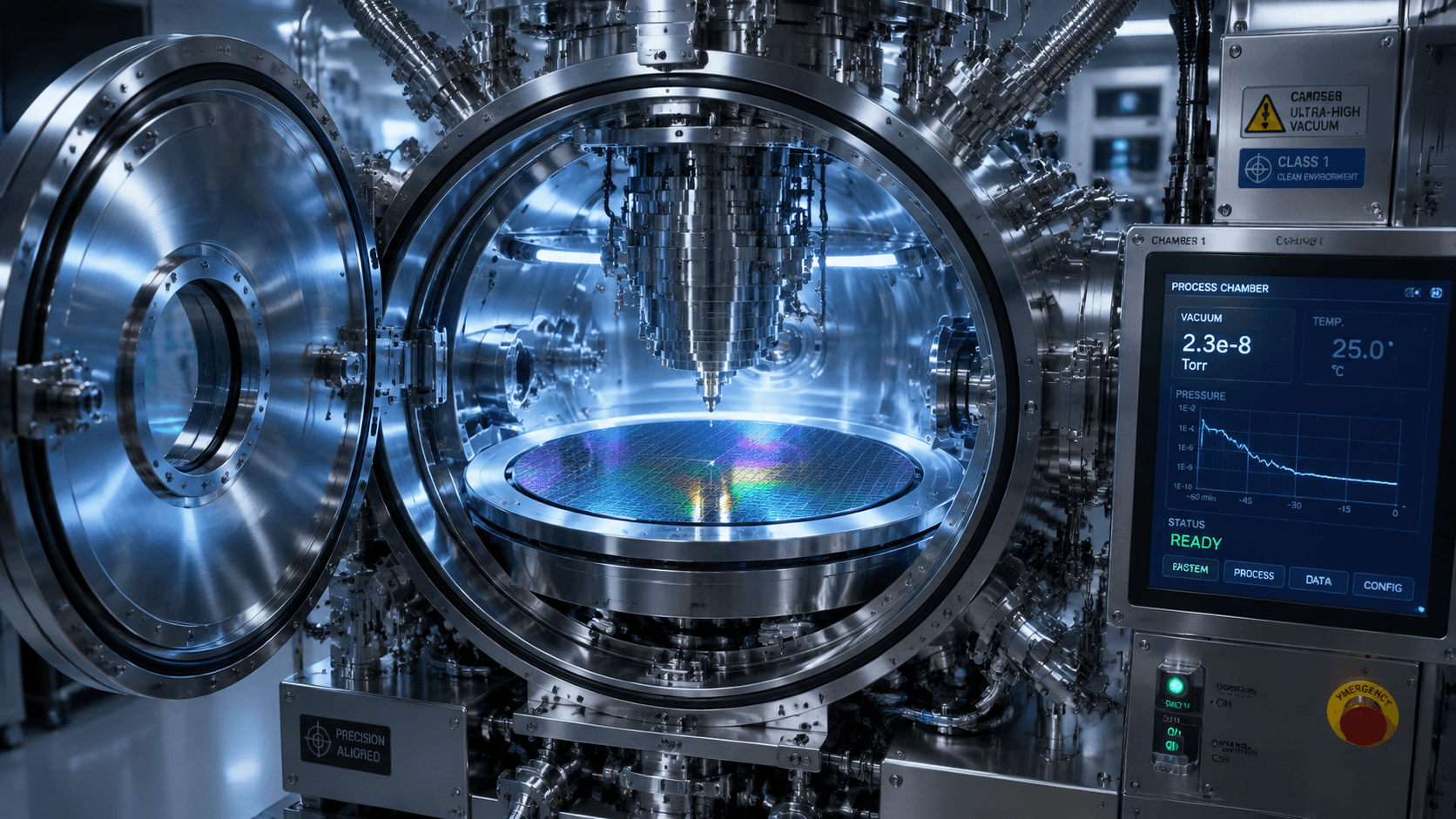
The production of modern semiconductors, from the historical demonstration of atmospheric pressure with Magdeburg hemispheres to cutting-edge EUV lithography, critically depends on creating and maintaining extreme vacuum environments. These specialized conditions are essential for preventing contamination by airborne particles, which can ruin delicate microelectronic circuits. Furthermore, achieving ultra-high vacuum levels allows for the precise etching of intricate patterns onto silicon wafers with sub-nanometer accuracy. This controlled environment is also vital for stabilizing the plasma used in various manufacturing processes, ensuring consistency and enabling the creation of the most advanced chips.
Without these extreme vacuum chambers, the precision, purity, and stability required for fabricating chips at the sub-nanometer scale would be impossible. The technology represents a fundamental, albeit often overlooked, pillar supporting the entire global semiconductor industry.
The reliance on extreme vacuum technology highlights a fundamental trade-off in advanced manufacturing: the pursuit of ultimate precision necessitates isolating processes from the ambient environment. As semiconductor features shrink to atomic scales, the sensitivity to external interference, even from single molecules, increases exponentially. This underscores a growing challenge in the AI era: scaling manufacturing capabilities while managing increasingly complex and fragile environmental controls. Future innovations may explore novel materials or process designs that are inherently more robust to contamination, potentially reducing the extreme infrastructure demands and associated costs, or alternatively, focus on more localized and efficient vacuum generation techniques.
AI-generated to prompt reflection — not editorial opinion, not advice, not a statement of fact. How this works.