Google Reportedly Designing 'Frozen v2' Chip with Gemini AI Architecture
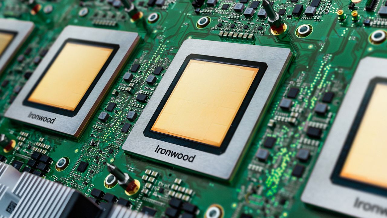
Google is reportedly developing a new server chip, internally codenamed "Frozen v2." This next-generation chip is designed to integrate a portion of the architecture of Google's Gemini AI model directly into its silicon. Engineers familiar with the project anticipate that this integration will lead to a significant performance improvement. Specifically, they project that Frozen v2 could achieve between 6 to 10 times more tokens processed per watt of energy consumed compared to Google's current Tensor Processing Units (TPUs). This advancement aims to enhance the efficiency and power of AI computations within Google's data centers.
The reported development of Google's "Frozen v2" chip, embedding Gemini's architecture into silicon, signifies a strategic move towards optimizing AI hardware for enhanced energy efficiency. By integrating AI model specifics directly into the chip's design, Google aims to reduce the computational overhead and power consumption associated with processing large language models. This approach could set a new industry benchmark for performance per watt, potentially lowering operational costs and enabling more widespread deployment of advanced AI capabilities. The projected 6-10x improvement suggests a significant leap in hardware-software co-design, aligning with the growing demand for sustainable and scalable AI infrastructure in the coming decade.
AI-generated to prompt reflection — not editorial opinion, not advice, not a statement of fact. How this works.