Huawei's Kirin 2026 Chip Features Novel 'Logic Folding' Design
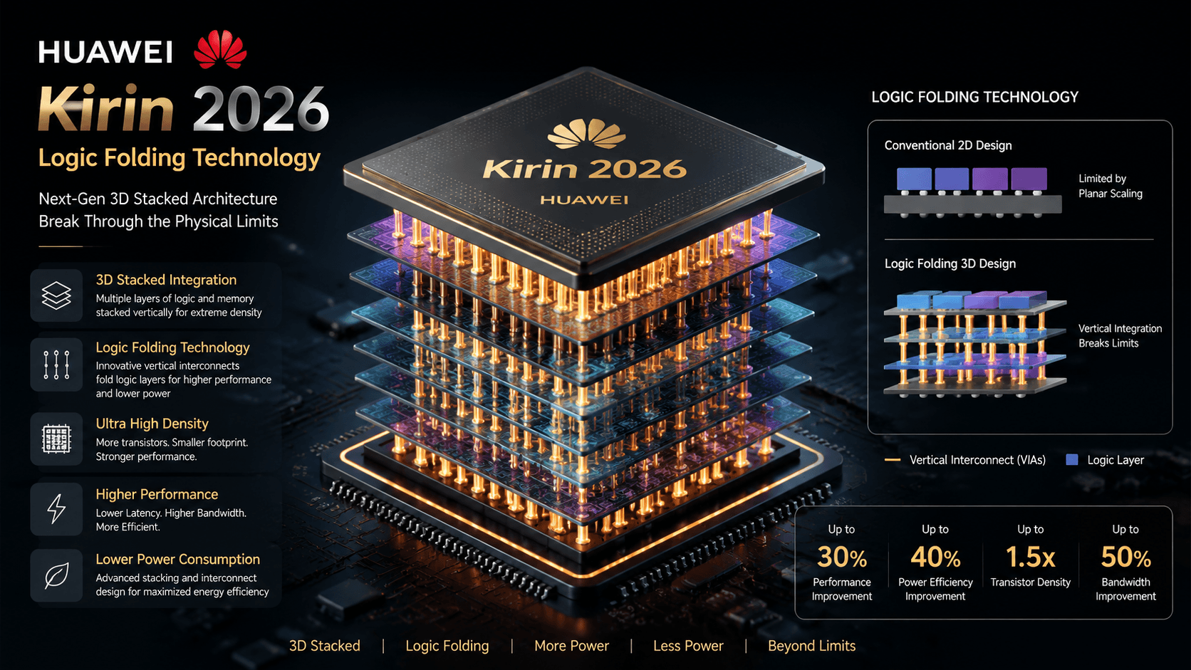
Huawei has unveiled details about its Kirin 2026 processor, which incorporates a new design principle termed 'Logic Folding.' This innovation, described in a paper by Tao's Law V2, allows for a significant increase in transistor density. The Kirin 2026 achieves a density of 175 million transistors per square millimeter (MTr/mm²). Notably, this advanced density has been realized without the use of extreme ultraviolet (EUV) lithography, a technology typically associated with cutting-edge chip manufacturing. The 'Logic Folding' approach appears to be a novel method for optimizing transistor placement and interconnects within the chip architecture. This development could have implications for chip design strategies, particularly for companies seeking to enhance performance and density while managing manufacturing costs or access to advanced fabrication equipment.
Huawei's reported breakthrough in transistor density for the Kirin 2026 chip, achieved through 'Logic Folding' without EUV lithography, suggests a potential shift in semiconductor design paradigms. This development could indicate that innovative architectural approaches can partially offset the reliance on the most advanced and capital-intensive lithographic processes. The long-term implications may involve a diversification of chip manufacturing strategies, potentially lowering barriers to entry for high-density chip production and influencing the competitive landscape by enabling more players to achieve significant performance gains. This also raises questions about the future trajectory of Moore's Law and the industry's ongoing pursuit of miniaturization and efficiency.
AI-generated to prompt reflection — not editorial opinion, not advice, not a statement of fact. How this works.