Intel Expands Photomask Production in California to Support Advanced Chipmaking
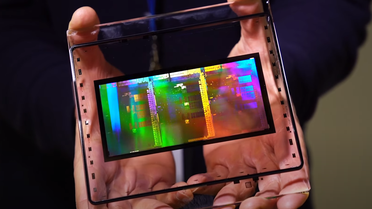
Intel has initiated an expansion of its Bowers Campus in Santa Clara, California, to increase its in-house production of photomasks. This strategic move is deemed crucial as semiconductor manufacturing processes become increasingly sophisticated. Photomasks are essential components in the lithography process, acting as stencils that define the intricate patterns on microchips. The expansion will focus on producing both Extreme Ultraviolet (EUV) and High-NA EUV photomasks. These advanced technologies are vital for manufacturing the next generation of smaller, more powerful, and energy-efficient processors. By bringing more photomask production in-house, Intel aims to gain greater control over its supply chain and ensure timely access to these critical components, thereby supporting its ambitious roadmap for future process technologies.
By investing in domestic photomask production, Intel is strategically de-risking its supply chain and enhancing its manufacturing autonomy, particularly for leading-edge EUV and High-NA EUV technologies. This move addresses the growing complexity and critical nature of photomasks in advanced semiconductor fabrication, aiming to mitigate potential bottlenecks that could hinder the deployment of new process nodes. Such vertical integration aligns with broader geopolitical trends emphasizing technological sovereignty and resilience in critical industries. The focus on EUV and High-NA EUV underscores the industry's trajectory towards ever-smaller feature sizes, presenting both opportunities for performance gains and challenges in manufacturing yield and cost management over the next decade.
AI-generated to prompt reflection — not editorial opinion, not advice, not a statement of fact. How this works.