Intel First to Mass Produce Logic Chips Using ASML's High-NA EUV Technology
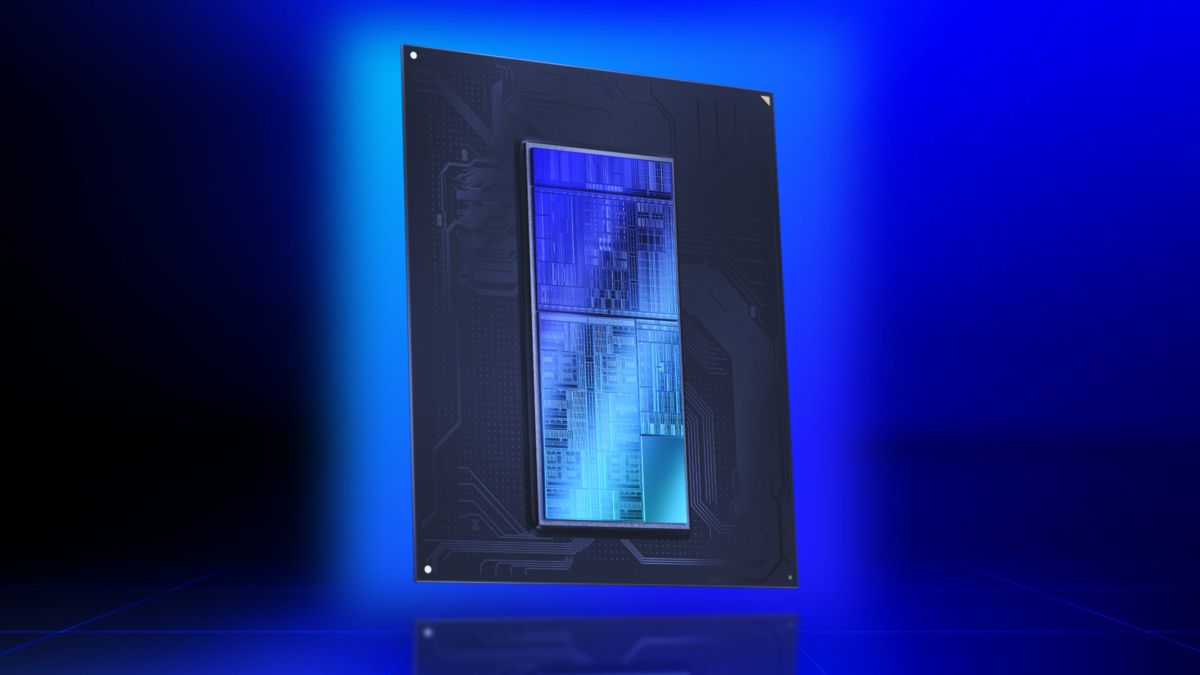
Intel has achieved a significant milestone by becoming the first company to ship high-volume logic chips manufactured with ASML's High Numerical Aperture (NA) Extreme Ultraviolet (EUV) lithography technology. Specifically, select layers of the upcoming Panther Lake processors are now dual-qualified for use with ASML's 0.55 NA scanners. This marks the initial deployment of this advanced lithography technique in high-volume production environments for logic chips. The successful integration of High-NA EUV tools by Intel signifies a critical step forward in semiconductor manufacturing capabilities. This advancement is expected to enable the production of more complex and powerful chips.
Intel's adoption of ASML's High-NA EUV technology for high-volume logic chip production represents a strategic investment in next-generation semiconductor manufacturing. This move positions Intel at the forefront of lithographic innovation, potentially offering a competitive edge in chip performance and density. The successful qualification of these advanced tools suggests a maturing ecosystem for High-NA EUV, which will be crucial for future technology nodes. As the industry navigates the increasing complexity and cost of chip fabrication, such technological leaps are essential for maintaining Moore's Law and driving advancements in computing power over the next decade. This development underscores the ongoing arms race in semiconductor technology, where access to cutting-edge manufacturing processes is a key determinant of market leadership.
AI-generated to prompt reflection — not editorial opinion, not advice, not a statement of fact. How this works.